PCB Repair Station Built on Highly Accurate Gantry Reduces Scrapped Boards

Time to Read: 4m 0s


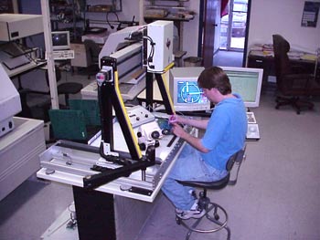
Now, using a highly accurate CNC Gantry, from Techno-isel, New Hyde Park, NY as the base platform, EPC's new computer-aided PCB repair system has significantly reduced scrapped boards. IBM, for instance, recovered the cost of the repair station in only six months from salvaging scrapped boards. EPC's new station, the Model 5500, projects any 'problem traces' onto the board with an LCD projector, which indicates the most likely areas or faults and it also detects recurring production errors. The Techno CNC Gantry allows the projected images from the LCD to be positioned with accuracy and precision that is essential in today’s densely packed PCBs.
EPC, Dallas, Texas, was founded in 1982 to produce products that aid circuit board manufacturers in the analysis and repair of errors. The company now offers a long list of tools for the electronic products industry including computer-aided repair systems, inner layer inspection tools, loaded board systems, and an audible resistance meter. EPC's customers range from Fortune 100 companies to the smaller, family-owned shops.
Old repair method
PCB manufacturers test finished boards for the soundness of the electrical connections on a device called a bed-of-nails tester. The bed-of-nails is a test fixture that has probes (that resemble nails) arrayed so that each will contact a grid point on the board simultaneously. The fixture is connected to automated test equipment that is programmed to iteratively check each network for opens and shorts. If a board fails, the test system produces a report indicating where the short is located. "The report gives two x-y coordinates," explains Evan Evans, engineering manager at EPC. "For example, it might say that the nail at point X23, Y19 shorted to the nail at point X99, Y87." In the past, repair technicians took the artwork used to create the board and identified the two traces involved in the short. Then they followed them on the actual board to find where the two wires might be touching. That was not difficult when boards consisted of just a single layer and it was possible to see entire traces by turning the board from one side to the other. After locating the problem spot, the technician scratched it with an exacto knife to break the connection. But as circuit boards grew more complex, it became impossible to follow the traces visually. "In today's multi-layer boards, traces go in one hole, then wander all through the inside of the board before coming out the other side," says Evans.As Evans explains, PCB manufacturers do a lot of testing of inner board layers before they are sandwiched together, so the inner layers are good most of the time. "Eighty five to ninety percent of the shorts are on the outer layers," he says. "There are many more processes on those layers. Along with the etching, there is also soldering to create pads and electrical plating of through holes." But even when a problem is on the outside of the board and it should be possible to repair, if the technician can't follow the traces to find the short, he has to scrap the board. "These boards are designated as having internal shorts and scrapped," Evans adds. "When we asked one board manufacturer to show us all of its scrapped boards with internal shorts, we found that 65 percent of them weren't internal shorts at all. They were just a case of the technician not being able to follow the traces and find the fault."
The other limitation of the past repair systems was that they gave no indication to management of recurring problems. In one example, a company had been building a particular board for three years at 100,000 boards per year. They were unaware that one out of 12 boards was shorted in the same place because there were 20 different repair people and no way to compile their experience to find this sort of trend.
A better approach
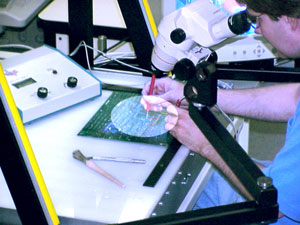
The Model 5500 is a significant improvement over the old repair methods because it addresses both limitations—the difficulty of following traces on multilevel boards and the inability to detect recurring problems. When a failed board is brought to this repair station, the operator enters the two x, y coordinates from the test report. The system's fault prediction software examines the CAD data used to manufacture the board and checks all of the pads and traces associated with the two coordinates to determine where the wires come in close proximity. When the fault prediction analysis is complete, the repair station uses a color LCD high-resolution video graphics projector to display repair data (traces, pads, components, and other information) directly onto the circuit board. The colors of the projected image can be changed so that there is maximum contrast between the circuit board and the graphic data.The system does not just display images, however. "It incorporates intelligence so that it actually walks the operator through the process," explains Evans. "The system highlights the first place to put the test probe, then the second place. It presents the problem areas one after the other so the operator can find the fault." The failure analysis software takes into account whether there might be internal shorts so the repair person does not waste time repairing these external faults only to find that the PCB must be scraped because of a non-repairable fault. A stereo zoom microscope is included as part of the Model 5500 so that location, verification, and repair of very small faults that could not be seen by the naked eye can be performed on the repair station. The repair station also features fault ranking software that collects a history of the faults that are reported and uses this historical data to determine the reparability of subsequent PCBs.
A key feature of the system is the accuracy with which it displays the images of the traces, pads, and so on. Positioning accuracy is critical because of the close proximity of the traces and components on today's PCBs. In designing the Model 5500, EPC had the option of building a gantry system on which to hand the LCD projector and the x, y positioning system. "We had designed many such mechanisms in the past but decided not to reinvent the wheel this time," says Evans. An advertisement in a trade journal convinced them to use a Techno Gantry System III.
This servomotor controlled gantry system delivers 0.0005-inch resolution and repeatability, and 0.003 inches/foot absolute accuracy. It is constructed on steel stress-relieved bases with hardened steel linear ways. Its shaft-and-bearing system produces very smooth, play-free motion and is an extremely rigid system that produces high-accuracy positioning. The gantry's design includes heavy cast aluminum side plates supporting the y axis, giving extra stiffness for accuracy in positioning. Anti-backlash ball screws and nuts are standard. These screws have excellent power transmission due to the rolling ball contact between the nut and screws, and this type of contact ensures low friction, low wear, and long life.
The Techno gantry comes in a wide range of work surface sizes. This allows EPC to offer its repair system in different sizes as well. There are three versions of the Model 5500, built on three different models of the Techno gantry. The EPC 5500 – 027 has an active board area of 21.5 inches by 22.0 inches (54.6 cm by 55.9 cm) and can repair a board of 32.0 inches by 27.0 inches. The EPC 5500 - 054 has an active board area of 40.0 inches by 22.0 inches (101.6 cm by 55.9 cm), allowing a board of 64.0 inches by 27.0 inches (162.6 cm by 68.6 cm) to be repaired. The EPC 5500 - 130 has an active board area of 50.0 inches by 42.0 inches (127 cm by 106.7 cm). It can handle boards of 64.0 inches by 47.0 inches.
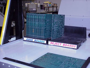
The Model 5500 is new but several companies are already using it with excellent success. IBM, as one example, recovered enough failed boards in the first six months of using the Model 5500 to pay for the system. Another example is the company that was producing hundreds of thousands of boards with one out of 12 being defective. This manufacturer used the system's fault ranking software to statistically analyze the historical repair data. This enabled them to find the source of the problem, a smudge in the original artwork that was creating a bridge across two traces. That single find alone went a long way toward paying for the system.
The Model 5500 offers PCB manufacturers a significant improvement over past repair methods. By helping technicians find more fixable faults, it reduces the number of scrapped boards. And by allowing manufacturers to see trends in failed boards, it helps fix production problems before they cause failed boards. A highly accurate gantry system ensures that the Model 5500 has the necessary precision to accommodate today's densely packed PCBs.
For more information contact: Techno, Inc. Linear Motion Systems, 2101 Jericho Turnpike, New Hyde Park, NY 11040. Phone: 516-328-3970 Fax: 516-358-2576 E-mail: TECHNO LINEAR MOTION SYSTEMS.


